UV‑LED Curing Technology for Semiconductor Packaging and Microchip Assembly
News 2026-09-23
As semiconductor chips become smaller and more integrated, advanced packaging processes such as flip‑chip, fan‑out and wafer‑level packaging set higher standards for adhesive curing. Tiny solder bumps, thin silicon dies and sensitive micro‑circuits cannot withstand high‑temperature thermal shock. Even a small temperature spike may lead to chip warpage, solder joint oxidation or hidden internal stress, reducing product yield and service life. For many chip manufacturers, curing quality directly determines the reliability of finished semiconductors.
In semiconductor workshops, UV curable adhesives are widely used for multiple key steps: flip‑chip underfill encapsulation, die attach bonding, component sealing, and thin conformal protective coating. These adhesives need full cross‑linking without bringing extra heat load to precision chips. Older mercury lamp UV curing systems have been gradually phased out in high‑end fabs. Mercury lamps generate massive infrared radiation alongside UV output. When irradiating micro‑chips, surface temperature rises sharply within seconds. Local overheating creates bubbles and micro‑voids inside thin underfill glue, which will turn into hidden failure points under temperature cycling test.
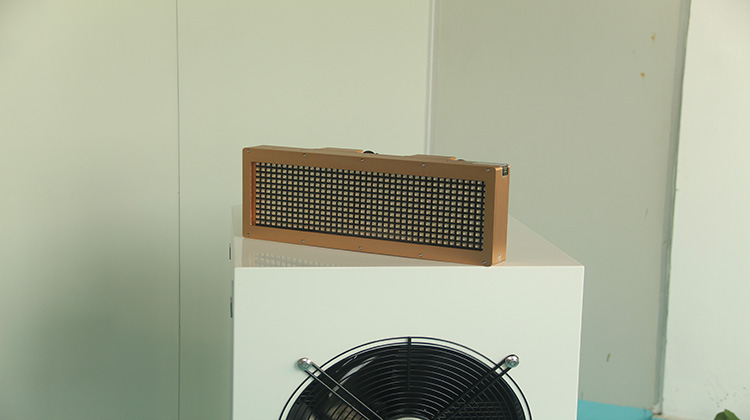
UV‑LED cold light curing solves these critical pain points for semiconductor production. Different from broad‑spectrum mercury lamps, LED‑UV equipment outputs targeted single‑wavelength ultraviolet light, with nearly no infrared heat radiation. The chip and substrate stay at near‑ambient temperature during the whole curing cycle. Temperature rise can be controlled within 5℃ for most sensitive assemblies, protecting solder bumps, silicon wafers and delicate circuit structures from thermal damage.
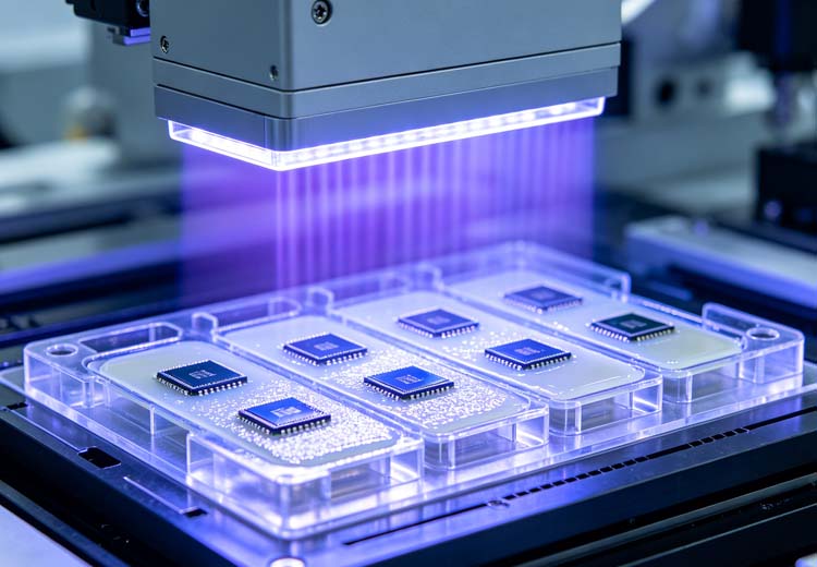
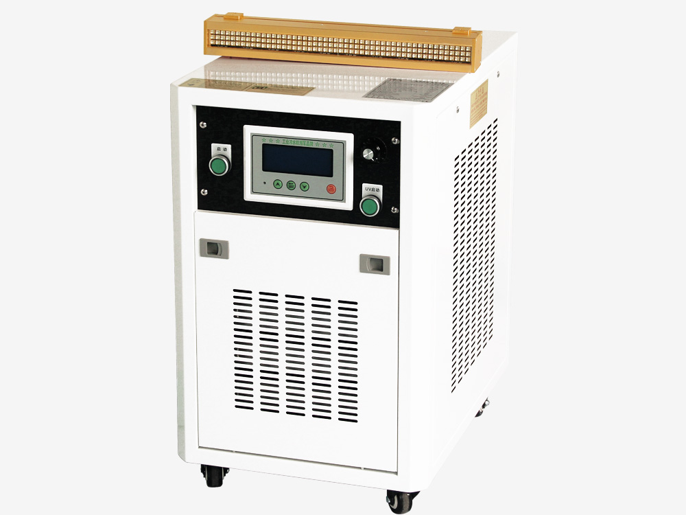
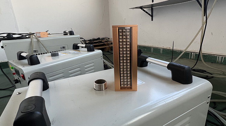
Uniform light output is another non‑negotiable requirement for semiconductor applications. Uneven UV dose causes partial incomplete curing, creating weak bonding points inside underfill layers. Large‑area water‑cooled LED‑UV curing lamps offer consistent irradiance across the entire illumination area. For batch processing of multiple chips on conveyor lines, every component receives stable UV energy. The adhesive cures evenly from surface to deep layer, micro‑bubbles escape sufficiently before full cross‑linking, and the final glue layer keeps dense and void‑free, without hidden gaps between die and substrate.
Different semiconductor processes have different wavelength demands. 365 nm is widely adopted for underfill and die attach adhesives, providing good penetration for thin glue gaps between chip and substrate. 385 nm and 395 nm are more suitable for protective coating and sealing applications. Factories can select matching wavelengths according to the photo‑initiator inside their UV adhesives, avoiding surface skinning while inner glue remains uncured.
Clean‑room compatibility makes water‑cooled LED‑UV lamps fit semiconductor production lines well. Instant on‑off function removes long warm‑up and cool‑down waiting time. Manufacturers can start curing immediately without preheating. Compared with mercury lamps, LED‑UV reduces power consumption greatly and contains no harmful mercury materials, meeting clean‑workshop environmental standards. For 24‑hour continuous automated packaging lines, stable light output avoids batch‑to‑batch quality fluctuation.
Even with excellent UV‑LED curing hardware, semiconductor engineers still need to tune light intensity, total energy dose and exposure time properly. Too low UV dose leads to incomplete cross‑linking and poor bonding strength. Excessive energy may trigger material brittleness. Shadow areas beneath chips also need attention; for these positions, manufacturers usually adopt dual‑curable UV‑thermal adhesive to complete full curing after UV exposure.
In summary, low‑temperature, high‑uniformity LED‑UV curing has become an essential technology for modern semiconductor advanced packaging. It prevents thermal‑induced chip damage, reduces void and bubble defects in underfill glue, raises production yield, and guarantees stable performance of microchips in long‑term temperature cycling. As chip integration keeps increasing, UV‑LED cold‑light solutions will gain wider adoption across semiconductor assembly and packaging workshops.